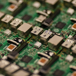
Before delving into the manufacturing process, let’s clarify what a PCB is. A PCB, or printed circuit board, serves as the backbone of almost all modern electronic devices. It provides mechanical support and electrical connections among electronic components through tracks, pads, and other features etched from copper sheets laminated onto a non-conductive substrate.
PCBs come in various types and complexities, from simple single-layer boards used in consumer electronics to intricate multi-layer boards found in advanced computing devices.
PCB Manufacturing Steps
1. Design and Schematic Capture:
The initial step involves translating the circuit schematic into a PCB layout.
Software tools like Altium Designer or Eagle are commonly used for this purpose.
2. PCB Fabrication Process:
Starts with selecting the appropriate substrate material based on the application.
Copper layers are applied to the substrate and then etched away to create the desired circuit patterns.
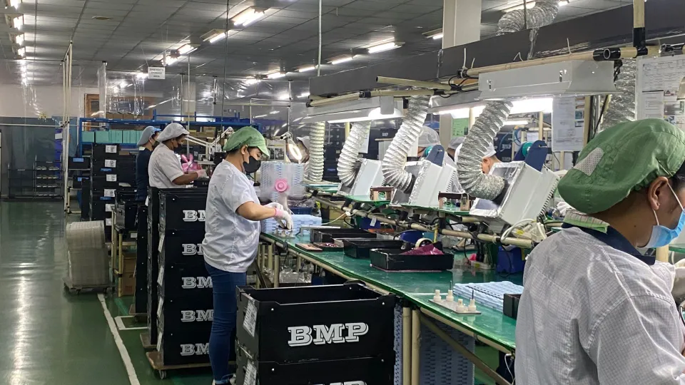
3. PCB Assembly Process:
Involves automated machines placing surface-mount devices (SMDs) onto the PCB.
Through-hole components are inserted manually or by automated insertion machines.
4. Testing and Quality Control:
Various testing methods such as in-circuit testing (ICT) and functional testing are employed.
Inspections ensure that the PCB meets performance and reliability standards.
Types of PCBs
PCBs come in various types, each tailored to specific needs based on complexity, materials used, and intended application:
Single-layer PCBs: Basic designs with a single layer of substrate and copper.
Double-layer PCBs: More complex designs with two layers of substrate and copper traces.
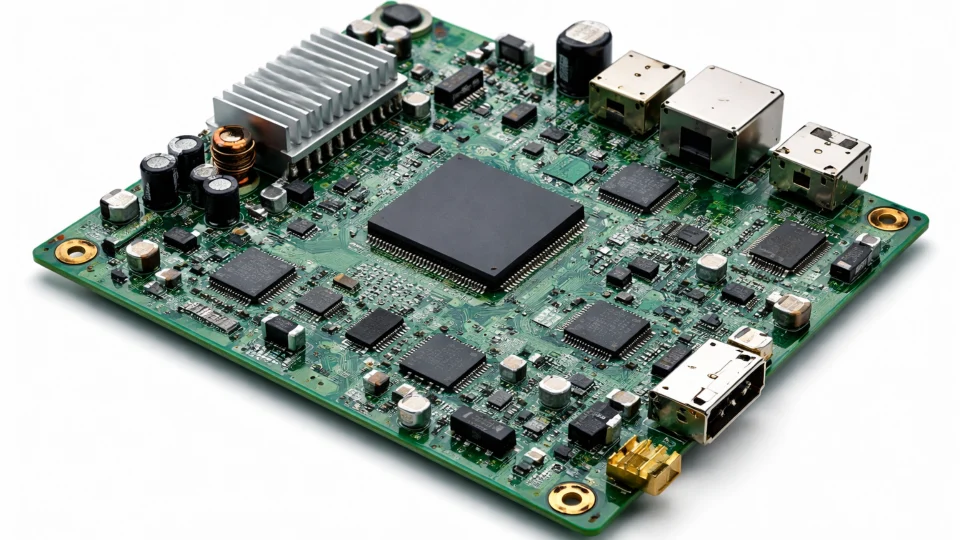
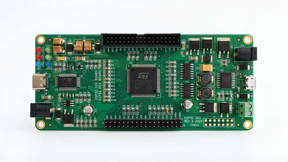
Multi-layer PCBs: High-density designs with multiple layers (4 layers or more) interconnected via vias.
Conclusion
In conclusion, manufacturing a PCB is a highly intricate and precise endeavor that blends art and science. Each step—from initial design to final inspection—requires careful attention to detail and adherence to rigorous quality standards. As technology advances, so too does the sophistication of PCB manufacturing, enabling the creation of smaller, more powerful, and more reliable electronic devices.
PCBs primarily use materials such as FR4, which is a type of fiberglass-reinforced epoxy laminate. Other materials include metals like copper for conductive traces, solder masks for insulation, and various chemicals for etching and plating.
How long does it take to make a PCB?
The time taken to manufacture a PCB depends on factors like complexity, order volume, and the manufacturer's production capacity. Typically, it can range from a few days for simple prototypes to several weeks for complex multi-layer boards.
What are the common challenges in PCB manufacturing?
Common challenges include ensuring precise alignment of layers during lamination, controlling the quality of plated-through holes, managing thermal expansion differences in materials, and maintaining consistent quality across large production runs.
What is the future of PCB manufacturing?
The future of PCB manufacturing is driven by trends towards miniaturization, increased complexity, and environmentally friendly processes. Technologies like additive manufacturing (3D printing), flexible PCBs, and embedded components are likely to play a significant role.
Stay Tuned!Unlock key insights in our upcoming post as we examine the challenges the Philippines faces in rising as a global powerhouse in SMT PCB assembly. Subscribe now and stay ahead of the curve!